The Semiconductor Race – India’s Quest for Technological Sovereignty in a Fragmented Global Order
February 03, 2026 Rajas Purandare
Abstract –
The global semiconductor race has emerged as a defining feature of the 21st century’s technological and geopolitical landscape. Amid escalating U.S.-China rivalry and supply chain disruptions, semiconductor manufacturing has become a symbol of economic security and strategic autonomy. The article examines how India can transition from a digital consumer to a digital producer in its pursuit of technological sovereignty through its emerging semiconductor policy architecture and analyses its prospects.
It explores India’s Production Linked Initiative (PLI), foreign partnerships, and strategic positioning in Indo-Pacific’s techno-economic networks. By situating India’s semiconductor ambitions within global supply chain realignments, the article tries to evaluate how India can architect its policies and rise as a semiconductor power.
Keywords- Semiconductors, U.S.-China, technological sovereignty, supply chain
Research Questions –
Eurasia Group’s "The Geopolitics of Semiconductors" (2020) provides one of the most comprehensive analyses of how the semiconductor industry has become a central axis in U.S.-China strategic competition. The report highlights that semiconductor manufacturing has become increasingly concentrated within a few geographies, primarily Taiwan and South Korea, creating both economic efficiencies and acute geopolitical vulnerabilities.
The study identifies semiconductors as a strategic bottleneck for China, noting that despite massive state investments exceeding $200 billion through the National IC Investment Fund, China remains technologically dependent on foreign producers, such as TSMC, Samsung, and Intel.
The IDTechEx report “Strategic Silicon: Geopolitics is Redirecting Semiconductor Investment” (Chag, 2025) provides an analysis of how intensifying geopolitical rivalries are reshaping the global semiconductor landscape. The study emphasises that semiconductors have transitioned from being primarily economic goods to becoming instruments of national strategy, sovereignty and technological power.
With over 90% of the world’s most advanced chips produced by Taiwan Semiconductor Manufacturing Company (TSMC), the report identifies Taiwan as both a core and a vulnerability of the global semiconductor ecosystem. Rising tensions in the Taiwan Strait have heightened global anxieties over supply chain resilience and technological dependency.
The article highlights a surge in semiconductor reshoring initiatives across major economies. Between 2024 and 2025, over USD 480 billion in investments were announced in the U.S. alone, driven largely by the Chips Act and joint ventures involving TSMC, Bosch, Infineon, and NXP, signalling the continent's ambition to restore semiconductor sovereignty. Similarly, Japan, South Korea are bolstering their domestic ecosystems through state-backed investments, with Japan’s Rapidus aiming for 2nm production by 2027.
Chang (2025) concludes that the semiconductor supply chain is undergoing a structural realignment, transitioning from a globalised system driven by efficiency to a regionally anchored network governed by security and strategic autonomy.
The report situates this transformation within the broader context of techno -nationalism and economic decoupling, where semiconductors are viewed as strategic silicon, central to both industrial competitiveness and geopolitical leverage.
The report “Semiconductor Technology Competition Seen Through Patent Analysis” (Ishiguro 2025) analyses global semiconductor rivalry through the lens of intellectual property. It highlights how semiconductors have become strategic assets closely tied to national security and geopolitical tensions, especially between the U.S. and China, reshaping global technology cooperation and supply chains.
Using the patent data, the report identifies differences between the U.S. and China in their approaches to innovation. U.S. companies such as Synopsys and Cadence emphasise open innovation, frequently referring to international patents and technologies, whereas Chinese firms and institutions like the Chinese Academy of Sciences and NAURA Technology Group focus heavily on domestic patent development. This suggests China’s strategy centres on building technological independence, while U.S. cooperation relies on global cooperation and licensing.
The report concludes that patents are now a central element of semiconductor strategy. They serve not only as protection for innovation but also as a means of managing geopolitical risks and forming international partnerships. It argues that the semiconductor industry is entering a phase of “technological decoupling” where U.S. and Chinese firms follow divergent innovation models – one open and collaborative, the other domestically concentrated. For other countries, the study emphasises the importance of maintaining a balanced relationship and using IP strategically to reduce overdependence on any single power.
Bhandari (2023), in his paper, provides a detailed overview of how global semiconductor geopolitics are being reshaped by the growing strategic and technological rivalry between the U.S. and China. The study traces the origins of the semiconductor shortage to factors such as the COVID-19 pandemic, natural disasters and most importantly, U.S. export control measures on advanced technologies to China.
These measures were first introduced under the Trump administration and expanded under the Biden administration, have triggered a broader technological decoupling, where both countries are striving for self-sufficiency in critical technologies.
The paper highlights how the semiconductor supply chain, once globalised and efficiency-driven, is now becoming fragmented due to national security concerns. The U.S. CHIPS and Science Act and China’s Made in China 2025 initiative illustrate the competing approaches towards technological security leadership. Bhandari distinguished between “fragmentation by default, which occurred in semiconductor manufacturing, spread across East Asia in the late 20th century, and “decoupling by design”, which now reflects deliberate state-led efforts to localise and control supply chains.
Finally, the paper examines India’s position within the evolving order. It argues that India is strategically trying to balance between blocs by promoting domestic semiconductor production while maintaining multiple partnerships under frameworks like friend-shoring. India’s semiconductor mission, design-linked incentives, and emphasis on secure and trusted supply chains demonstrate its aspiration to integrate into the global value chain while safeguarding national interests.
Introduction –
Semiconductor chips are foundational components of nearly all modern electronic devices, ranging from smartphones to computers to critical military and industrial systems. They are composed of semiconductor materials- primarily silicon, crafted to control electrical currents precisely. This level of precision enables complex data processing and control functions at microscopic scales.
A semiconductor chip consists of billions of tiny transistors on a small silicon wafer, acting as the essential building blocks for integrated circuits. The architecture and manufacturing process allow them to act as either conductors or insulators, depending upon the needs of the circuit, driving advancements in information technology since the mid-20th century.
Semiconductors advance critical sectors like AI, defence systems, industrial automation, and emerging technologies, making them a technological and strategic “chokepoint” at the global level.
The semiconductor ecosystem comprises various types of chips, each serving a distinct yet complementary function within electronic systems. Logic chips are designed to process data and execute instructions, forming the computational core of devices such as smartphones, computers, AI systems and military technologies. They determine how data is manipulated, enabling functions like decision-making and complex calculations.
Memory chips, on the other hand, are responsible for storing and retrieving data for processing, and they include various subtypes such as DRAM (Dynamic Random Access Memory and NAND flash memory used in data centres, servers, and consumer electronics.
Analog chips provide a wide range of functions, including working with sensors to convert and modify analog signals (e.g., temperature, speed, and pressure, which can span a range of continuous values) into digital signals used by computers (i.e., discrete values made up of 0's and 1's).30 Analog chip applications also include power management designed to convert, control, and distribute electrical power (e.g., AC to DC power conversion) in, for example, electric vehicles. Analog chips also are used for communications, including mobile phones (e.g., 5G, Bluetooth, wireless connectivity) and military detection and surveillance equipment (e.g., radar, sonar, infrared imaging).[1]
Optoelectronics, Sensors, Discretes (OSD), Optoelectronic semiconductors are used to interact with or produce light. The largest applications markets for optoelectronics include light-emitting diodes (LEDs); image sensors, such as those used in cameras, and laser diodes, such as those used in fibre optic communications.
Other sensor applications include semiconductors (often integrating analog components) designed to detect or control properties such as temperature, pressure, and acceleration. Sensors have a wide array of applications in consumer electronics (e.g., mobile phones, vehicles, and industrial equipment).
Discrete semiconductors typically perform a single electrical function—for example, controlling electric current in an integrated circuit. These types of semiconductors are typically produced using mature node technology.1
The geopolitics of semiconductors is characterised by intense strategic competition, primarily between the U.S. and China, with other actors, such as Taiwan, South Korea, the EU, and emerging powers like India, also shaping the technology. Semiconductors are essential for everything from consumer electronics to high-end military systems, making control over their supply and innovation a matter of national security for major powers. The U.S. dominates design, Taiwan and South Korea lead advanced chip fabrication, and the EU’s ASML has a monopoly on critical lithography equipment needed for cutting-edge chips.
U.S.–China Semiconductor Race for Supremacy –
The U.S. has established itself as a leader in semiconductor innovation, with companies like Intel, Nvidia, and Qualcomm driving technological advancements. However, it heavily depends on advanced chip manufacturing capabilities, such as those of Taiwan’s TSMC and South Korea’s Samsung. To reduce this, the U.S. has enacted the CHIPS and Science Act, which aims to strengthen domestic chip manufacturing and enhance national security. Additionally, the U.S. is forging technical partnerships with Japan, the Netherlands and other key allies to limit China’s access to essential semiconductor technologies.
The current Trump administration has been focusing on pushing the same goals promoted by Biden, but more aggressively. As of August 2025, Trump announced a 100 per cent tariff rate on foreign semiconductors, while companies that establish research or manufacturing operations in the US would be exempt from these tariffs. However, they might still face tariffs if they fail to fulfil their investment commitments.[2]
The Trump administration also incentivised manufacturers to build plants domestically.[3] On 1 July, the administration proposed increasing federal tax credits for eligible semiconductor firms from 25 per cent to 35 per cent for domestic projects.
The administration recently established a new entity, the US Investment Accelerator, to take charge of the Chips Act programme and accelerate corporate investments within the United States.
This body is responsible for overseeing the execution of the Chips and Science Act. The initiative aims to motivate companies to invest heavily in the US by streamlining regulatory requirements, expediting the permitting process, coordinating efforts among federal and state agencies, enhancing access to national resources, and helping cut fab costs in the US by as much as 10 per cent. [4]
The U.S. has adopted a multidimensional strategy to reduce China's dependence on the global semiconductor ecosystem. Through a combination of export controls, industrial policy and alliance coordination, the U.S. seeks to constrain Beijing's access to advanced technologies.
The U.S. has further consolidated this effort through coalition-based technology containment, enlisting allies like the Netherlands and Japan to block critical lithography exports. Complementary financial and investment regulations now restrict U.S. capital and expertise from flowing into sensitive Chinese sectors, reinforcing a techno-industrial decoupling.
China aspires to produce 75% of the semiconductors domestically but remains heavily dependent on foreign technology, occupying a much smaller share of global chip design and advanced foundry capacity.
In retaliation for U.S. export controls, China has restricted exports of essential minerals such as gallium and germanium, upon which the global semiconductor industry depends. China is also accelerating investment in domestic innovation and nurturing new champions in chip design and fabrication.
Despite huge investments, China still faces gridlock, especially in electronic design automation (EDA) tools and cutting-edge lithography, largely monopolised by Western firms. The rivalry has reconfigured the entire global semiconductor supply chain, pushing countries and companies to diversify sources, reshape trade relations and build new production platforms.
Economies in Asia and Europe now seek to reduce over-reliance on either power while price spikes and supply disruptions complicate access to advanced chips and key materials across industries.
India’s Semiconductor Gambit –
In 2022, India launched the India Semiconductor Mission (ISM). The policy aims to develop national capabilities and strategically position India within the global value chain across the design, manufacturing and assembly and packaging segments.[5] The ISM also aims to combine innovation and industrial policy through its focus on R&D, human resource development, and incentivising private companies.
Building national capabilities across public and private institutions is key to unlocking economic value from industrial policies.[6] At the time of ISM’s launch in 2022, the Indian semiconductor market was valued at US$26.3 billion and was projected to increase to US$271.9 billion at a CAGR (Compound Annual Growth Rate) of 26.3 per cent by 2032. [7]
The Indian semiconductor market is set to achieve a valuation of US$55 billion by 2026, according to a report from global consultancy firm Deloitte.The report states that more than 60% of the semiconductor market in India will be driven by three industries: smartphones and wearables, automotive components, and computing and data storage. The industry is expected to play an important role in enhancing the global value chain, expanding to a market size of US$85 billion and generating employment for 600,000 people by 2030.[8]
India’s approach emphasises technology transfer and global partnerships. Landmark collaborations with the U.S., Japan and leading chipmakers are fostering workforce development, sharing of best practices and co-funding of research in advanced packaging design and fabrication. The India- U.S. Initiative on Critical and Emerging Technology (iCET) exemplifies this international approach, aiming to build resilient supply chains and a competitive domestic ecosystem.
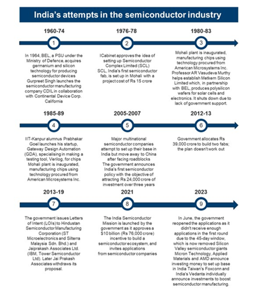
Image Credits - https://ibef.org/blogs/india-s-emergence-as-a-semiconductor-manufacturing-hub#:~:text=Semiconductor industry in India - An overview,26.3% to US$ 271.9 billion by 2032
During Semicon India 2025, the Indian Space Research Organisation (ISRO) unveiled its indigenously developed next-generation microprocessor that is set to revolutionise Indian space missions. Called the Vikram 3201, this microprocessor is based on the 32-bit architecture and is set to give a major boost to spacecraft technology from ISRO.
Vikram-32 is the successor to the VIKRAM160 – a 16-bit microprocessor that has powered ISRO's launch vehicles since 2009. A “Make-in-India” version of the VIKRAM1601 processor was subsequently inducted in 2016 after the 180nm semiconductor fab was established at SCL.
VIKRAM3201 & the VIKRAM1601 have a custom Instruction Set Architecture, with floating-point computation capability and high-level language support for the Ada language. All the software tools, such as the Ada compiler, assembler, linker, and simulator, along with the Integrated Development Environment (IDE), are developed in-house by ISRO.
The initial lot of VIKRAM3201 devices was successfully validated in space in the Mission Management Computer of the PSLV Orbital Experimental Module (POEM-4) in the PSLV-C60 mission. These microprocessors have been designed & developed by the Vikram Sarabhai Space Centre of ISRO in collaboration with SCL.[9]
Unlike commercial processors, space processors must endure harsh environments like extreme cold, heat, radiation and stress during launches. The 180nm node provides enhanced radiation tolerance, reducing the risk of total ionising dose damage and bit flips, making it suitable for avionics guidance and onboard control systems. Since launch vehicles and satellites require deterministic performance rather than sheer clock speed, ISRO has prioritised robustness and consistency over miniaturisation.
India is also part of the Quad’s Semiconductor Supply Chain Contingency Network, which facilitates coordination among Quad countries in securing and ensuring resilient supply chains.69 Potential partnerships were underway in the form of capability assessments under the CHIPS 13 Act’s International Technology Security and Innovation (ITSI) Fund.
Even though the future of the CHIPS Acts is uncertain under the Trump administration, commitment towards partnerships on semiconductor research and supply chain diversification remains a key component of US-India technology relations under the 2025 Joint Leaders’ Statement. These developments unfold amidst talks of the first US-India defence semiconductor fabrication unit coming up in Uttar Pradesh, which would make India one of the few countries, apart from China, to have manufacturing capabilities in complex compound semiconductors in the Indo-Pacific.
Japan was the second Quad member after the US to sign an agreement for the joint development of the semiconductor ecosystem in India.73 Similar agreements exist with the EU to promote knowledge exchange, innovation, R&D, and “robust supply chains. (Nandi, A. 2025).
India’s Manufacturing First Strategy –
Rewards of the Strategy –
Limits of the Strategy –
Challenges to India’s Semiconductor Development –
India’s approach to semiconductor development reflects a hybrid strategy that combines domestic capacity-building with international technological partnerships. The establishment of facilities such as CH Power’s Sanad assembly and testing unit, and the Micron and Tata-Powerchip Semiconductor Manufacturing Corporation collaborations in Gujarat exemplify this dual track of industrial expansion and foreign technology integration.These partnerships provide critical access to manufacturing expertise and process know-how, but simultaneously underscore India’s continued dependence on external technology ecosystems.
Despite these limitations, India contributes nearly 20% of the global semiconductor design talent, and under the Design Linked Incentive (DLI) scheme, 23 design projects have been approved, indicating strong upstream capabilities in chip design and innovation. However, Kaur (2025) notes that design competence does not equate to fabrication expertise, as manufacturing requires precision engineering, high–yield process control, and complex supply chain integration.
The government has taken notable steps to address the human capital deficit, with over 60,000 engineers trained in semiconductor-related domains. Yet, the industry estimates suggest that this represents only a fraction of the specialised workforce required to sustain large-scale production.
Moreover, the capital intensity of semiconductor fabrication often exceeds US$10 -20billion per facility, posing significant financial and operational challenges. This economic barrier is compounded by the technological learning curve, which can take years to achieve in international competitiveness through yield optimisation and quality assurance.
S Shivkumar and S Sharma, in their article entitled “Semiconductor Clusters in the Making: India’s Push for Global Competitiveness”, discuss that despite significant advancement, design capabilities and attractive incentives, India needs to tackle several issues such as infrastructure deficits, dependencies in supply chains.
1. High Infrastructure Prerequisites- Semiconductor fabrication: It requires precision-grade facilities, uninterrupted high-voltage power, and large volumes of ultrapure water, Class 1 cleanrooms, and specialised transport and logistics. Semiconductor Clusters in the Making: India’s Push for Global Competitiveness and Networks for Sensitive Equipment. In India, these capabilities are unevenly distributed, with only a handful of industrial zones approaching “fab-ready” standards.
2. Supply Chain Dependence: India currently lacks domestic production capabilities for essential semiconductor inputs, such as high-purity chemicals, speciality gases, silicon wafers, and ultrapure water, resulting in over 90 per cent of these inputs being imported. This reliance increases costs, lengthens lead times, and exposes Indian projects to geopolitical supply shocks.
3. Skilled Workforce Shortages in Manufacturing: India’s semiconductor ambitions face a significant manufacturing talent gap despite the country producing roughly 600,000 electronics-related engineering graduates annually. Only a small fraction, around one per cent, possess the specialised capabilities needed for fabrication, advanced packaging, and precision equipment maintenance without extensive retraining. Industry estimates project a shortfall of 250,000–300,000 skilled professionals by 2027, highlighting a structural constraint on scaling production capacity.
4. Weak R&D and Innovation Ecosystem: A deeper challenge is India’s underdeveloped research and innovation base. The country spends just 0.7 percent of GDP on R&D, far below the United States (3.6 percent) and China (2.4 percent). Corporate R&D intensity is especially low: India had only 15 firms among the world’s top 2,000 corporate R&D spenders in 2023, with combined investments of $5.9 billion—less than a tenth of Google’s annual R&D outlay. Universities, while producing a vast supply of engineers, publish relatively little world-class research and maintain weak industry linkages, raising concerns about whether India can generate the long-term process innovations that underpin advanced chipmaking. Without a robust R&D pipeline, India risks being confined to an assembly- and packaging-driven role, rather than evolving into a genuine technology originator.[12]
The Pragmatic Path Forward -
Escalating U.S.-China Tensions and diversification of global supply chains have created new opportunities for India, offering political stability and a skilled workforce. India can emerge as a serious contender in the high-stakes industry. India’s electronics exports surged by 47% year-over-year in Q1 FY26, driven by a remarkable 240% increase in smartphone shipments to the U.S., which now account for 44% of American smartphone imports. Vaishnaw also highlighted ongoing efforts to reduce India’s dependence on Chinese rare earth magnets, reflecting a broader strategy to strengthen the country’s role in advanced technologies.
These developments align with the U.S.’s intent to deepen ties with India as a critical partner in countering China, particularly in strategic sectors such as semiconductors, artificial intelligence, digital infrastructure, and resilient supply chains. [13]
India currently holds a significant position in the global semiconductor value chain, accounting for over 20% of the world’s chip design engineers.[14] By strategically prioritising backed processes such as Outsourced Semiconductor Assembly and Testing (OSAT) and Assembly Testing and Manufacturing (ATMP), India is well positioned to occupy critical supply chain segments before transitioning to advanced node manufacturing.
It is imperative that a comprehensive government-led initiative should facilitate the growth of indigenous R&D, promote technology transfer, support the creation of domestic intellectual property, and fund upcoming startups in the industry; these are fundamental to achieving authentic technological sovereignty. Substantial incentive schemes to promote more startups, regulatory simplification, and the establishment of a robust public-private partnership will further lower entry barriers for global investors while simultaneously fostering domestic innovation.
India’s phased semiconductor development strategy – beginning with legacy nodes and ATMP/OSAT (Assembly, Testing, Marking, and Packaging) before advancing into complex technologies like advanced packaging and compound semiconductors represents a sequencing that mirrors the path successfully taken by Taiwan and South Korea.
Phase 1 Dominating ATMP and OSAT (2025- 2030) –
India faces a big challenge with manufacturing, as it currently has only one large factory being built that will focus on older technology. Although there was a setback when the Vedanta Foxcoon project failed in 202, India has made some progress in the OSAT (Outsourced Semiconductor Assembly and Test) industry with the opening of the CG Semi facility. This is an important step toward becoming more independent in assembling and testing electronics.
As per a Times of India Report published on Jun 17, 2025, India’s first semiconductor unit is being constructed in Gujarat. As a part of this initiative, the state is facilitating the development of 1,500 residential units for expatriates and staff members of the Tata group and its vendors in Dholera, located in the Ahmedabad district. This fabrication facility is being built within the Dholera Special Investment Region and represents an investment of 91,000 crore. It is expected to generate skilled employment opportunities both directly and indirectly. [15]
Another report published by Economic Times on July 17, 2025, India’s Tata Electronics has agreed with German technology firm Robert Bosch GmbH to collaborate across various domains within the electronics and semiconductor sectors. As part of the Memorandum of Understanding (MoU), both companies plan to work together in advanced chip packaging and semiconductor manufacturing. The collaboration will focus on Tata Electronics' upcoming facility in Assam and its planned semiconductor foundry in Gujarat. In addition to semiconductor efforts, the two companies will jointly explore opportunities in local electronic manufacturing services, particularly in vehicle electronics. [16]
The central government has given approval to Micron Semiconductor for establishing a Special Economic Zone (SEZ) in Sanand, Gujarat. This SEZ, covering an area of 37.64 hectares, will be developed with an estimated investment of INR 130 billion (US$1.51 billion). The approval was formalized by the Ministry of Commerce through a gazette notification dated June 23, 2025. The ministry has also designated the SEZ as an Inland Container Depot under Section 7 of the Customs Act, 1962. This initiative is part of India’s broader strategy to attract high-value, capital-intensive investments in the semiconductor and electronics manufacturing sectors.[17]
Renesas Electronics, a Japanese semiconductor manufacturer, is in the process of establishing a new outsourced semiconductor assembly and Test (OSAT) facility in India. The pilot OSAT facility was inaugurated on 27th August 2025. This venture is a part of a collaborative effort with Murugappa Group from India and Stars Microelectronics from Thailand.
This new facility is projected to commence production of its first semiconductor chips by mid-2026. Additionally, a significant production plant is being constructed in Sanand, Gujarat, with an anticipated completion date of December 2026 and full-scale production slated to begin by October 2027.
India’s ATMP/OSAT sector is maturing through financed projects, global partnerships and strong government incentives. The focus is on backend semiconductor assembly and packaging is a proven path aligned with domestic industrial demand and international market dynamics. Although it still faces headwinds in technological upgrade, ecosystem depth and long-term global competitiveness. Addressing these gaps will be crucial towards a holistic strategic autonomy.
Phase 2 –
In the second phase, India’s semiconductor strategy must focus on moving up the value chain in two critical directions: advanced packaging and compound semiconductors (notably silicon carbide and gallium nitride. This approach targets high-growth sectors such as EVs, renewable energy and defence, aiming for greater technological autonomy.
India's Defence Research and Development Organisation (DRDO) has announced a significant milestone in semiconductor technology by developing indigenous methods for producing 4-inch SiC wafers and fabricating GaN HEMTs up to 150W.
A statement from the Indian Ministry of Defence said that these advancements, achieved by the DRDO's Solid State Physics Laboratory (SSPL), also include MMICs with power capabilities up to 40W, suitable for applications extending to X-band frequencies.
The establishment of indigenous GaN on SiC-based MMIC production has been successfully implemented at GAETEC (Gallium Arsenide Enabling Technology Centre) in Hyderabad. These technologies are considered essential for modern combat systems, radar technologies, electronic warfare, aerospace, satellite communications, and green energy initiatives.[18]
Gallium Nitrate is essential for AESA (Active Electronically Scanned Array) on fighter jets, e.g. Uttam and Virupaksha, as it significantly outperforms older technology of Gallium Arsenide by handling higher breakdown and voltage. In AESA radars, transmit/ receive modules require a high-power amplifier. GaN enables these amplifiers to generate more power output in a smaller space, which increases the detection range and signal of the radar.
GaN makes radar more effective and resistant to jamming, and it provides better thermal management and higher efficiency.
The higher power density of GaN allows T/R modules to be lighter and smaller, which is essential for modern platforms where weight and space are limited. Advanced radar systems integrated into smaller aeroplanes, drones and other mobile platforms without compromising performance because of weight and size reduction.
Agnit Semiconductors, based in Bengaluru, is positioning itself as a pioneer in Gallium Nitride technology, establishing India’s inaugural vertically integrated ecosystem encompassing wafers, devices and systems. The company was founded in 2019 by a consortium of researchers from the Indian Institute of Science and has been operational since 2021. The company is laser-focused on high-performance applications across critical sectors, including defence, aerospace, telecom, and power.
Agnit stands for Advanced Gallium Nitride Semiconductors, capturing both its technical focus and Indian roots. Derived from "Agnit", meaning "infinite," the name reflects the boundless potential of GaN technology in high-efficiency electronics.[19]
Agnit’s business model is distinctive, even on the global frontier, as it manages every aspect of the GaN value chain. This vertical integration allows for improving performance, characteristics, cost efficiency, and form factor optimisation right from the Inception Stage. Recent achievements highlight Agnit’s escalating prominence in the semiconductor domain. The company signed an MoU with the Ministry of Defence under the iDEX initiative to co-develop GaN RF transmitters. Additionally, it received the IESA Technovation Startup Award 2025, in the semiconductor category and secured the ELEVATE grant from the Karnataka government for indigenous technology advancement.
Field trials are currently underway with strategic partners, with volume production targeted within the next 12 months. Agnit has raised a total of $4.87 million to date, beginning with $1.3 million in angel funding in 2021 and followed by a $3.5 million seed round in 2024 co-led by 3one4 Capital and Zephyr Peacock. The funds have been deployed toward scaling GaN wafer processing, establishing pilot manufacturing infrastructure, and expanding into high-growth segments such as telecom and electric vehicles.18
Ind’s focus on advanced packaging and compound semiconductors reflects its frontline development of future chip technology, aligning with global trends and ensuring deeper integration into critical, value-added supply chain segments beyond legacy manufacturing.
The Alliance Ecosystem –
U.S. India -
The partnership between India and the U.S. on advanced semiconductor co-development is primarily anchored in the initiative on Critical and Emerging Technology (iCET) and the TRUST framework. Together, these initiatives foster strategic semiconductor collaboration aimed at enhancing national security, ensuring supply chain resilience and driving cutting-edge technological innovation.
President Biden and Prime Minister Modi announced the U.S.-India initiative on Critical and Emerging Technology (iCET) in May 2022 to elevate and expand our strategic technology partnership and defense industrial cooperation between the governments, businesses, and academic institutions of our two countries.
The initiative fosters Enhancing bilateral collaboration on resilient semiconductor supply chains; supporting the development of a semiconductor design, manufacturing, and fabrication ecosystem in India; and leveraging complementary strengths, both countries intend to promote the development of a skilled workforce that will support global semiconductor supply chains and encourage the development of joint ventures and technology partnerships on mature technology nodes and packaging in India.[20]
India - U.S. TRUST framework, launched in February 2025, serves as a successor to the iCET, deepening collaboration in critical areas in minerals, pharma, clean energy and space technologies in addition to semiconductors.
TRUST prioritises the establishment of trusted and resilient supply chains, along with coordination in industrial projects such as Micron's ATMP facility in Gujarat and advanced material supply networks. The initiative emphasises the co-development of innovation hubs, workforce training and harmonisation of standards crucial for the comprehensive growth of the semiconductor ecosystem in India.
India – Japan – South Korea Trilateral –
Tripathi (2025), in his article “Semiconductors as the Spark for an India-Japan-South Korea Trilateral, presents an argument for formalising a trilateral partnership between India, Japan and South Korea for semiconductor cooperation. Tripathi situates this proposal within the broader realignment of global technological supply chains amid U.S.-China tech rivalry.
Tripathi advocates for trilateral cooperation within a broader multipolar framework, as the U.S. seeks its decouple from China, Indo-Pacific countries such as India and Japan, and South Korea face both vulnerability and opportunity. The first India- Japan -South Korea Trilateral Policy Planning Dialogue (2024) is cited as a starting point. Tripathi contends that semiconductors can serve as the spark that accelerates the trilateral formation, given their focus on emerging technologies like AI,6G, IoT, EVs and quantum computing, all of which depend on chip access and innovation.
Japan possesses technological advancements and manufacturing capabilities in semiconductor materials, equipment and fabrication. Its strategy for Semiconductor and Digital Industries promotes strategic autonomy and comprehensive R&D across the supply chain.
South Korea dominates memory chip production, controlling over 60%of the world’s DRAM and NAND market, led by Samsung and SK Hynix. It’s “K semiconductor Belt Strategy and Special Act on National Technologies” that aims to consolidate Korea’s position as a leader in next-generation chips.
India presents an emerging market, focusing primarily on legacy node chips under the Semicon India Programme. Its advantage lies in its human capital, holding nearly 20% of global semiconductor design talent and its growing demographic dividend.
Lessons from the Global Arena –
India’s semiconductor strategy can gain significant insights from the global arena by benchmarking itself against Japan’s Rapidus consortium, the EU Chips Act and Vietnam's focus on capital development. Rapidus symbolises Japan’s ambitious initiative, supported by both government and private entities, in its advanced chip manufacturing industry with a goal of mass production of 2-nanometer logic chips by 2027.
The EU Chips Act is a key policy initiative that mobilises 43 billion euros to bolster Europe's semiconductor advancement through research, manufacturing and skills development. It mainly focuses on three pillars – Chips for Europe to foster R&D innovation, providing investment incentives aimed at enhancing chip manufacturing and supply chain resilience and facilitating coordination among member states and stakeholders through the European Semiconductor Board.
Vietnam’s national semiconductor strategy emphasises the importance of training and developing a strong semiconductor workforce, with the ambitious target of cultivating 50,000 qualified professionals by 2030 and a high-quality talent pipeline by 2050.
It is imperative that India foster and develop a deeper public-private partnership to effectively pool resources and implement complex technology projects. Drawing inspiration from EU chips, India should consider adopting a pillar approach that combines R&D innovation and extensive stakeholder coordination, combining government, private cooperation and academia.
India’s semiconductor initiative has the potential to accelerate decades of cluster development into just a few years by integrating global best practices tailored to India’s industrial landscape.
Hardware Trojans –
One of the major reasons for developing indigenous semiconductors is the threat of hardware Trojans made by foreign companies. Hardware trojans are a malicious modification implanted in semiconductors during the manufacturing process of an integrated circuit design or fabrication that alerts, behaves, leaks information, or degrades liability under certain conditions.
Kill switches are a type of hardware Trojan whose purpose is to degrade to disable a chip upon a specific command, effectively allowing remote shutdown or denial of service. Kill switches are also becoming a strategic tool that is being used by companies like ASML and TSMC to protect semiconductor intellectual property and prevent it from falling into hostile hands.
E.g. China being an authoritative regime and its growing semiconductor capacity, raises concerns regarding embedded vulnerabilities like hardware trojans in supply chain manipulation. Such risks force countries to semiconductor reshoring, developing indigenous semiconductor chips and adopt enhanced security measures to protect against espionage and technology sabotage.
Conclusion –
For India, semiconductors represent not only its technological prowess but also its economic resilience, national security and strategic influence in the region. A key driver for advancing India’s semiconductor mission is the development of ISM 2.0, envisioned as the cornerstone of a self-reliant ecosystem. Central to this strategy is the establishment of fab units to reduce import dependency, particularly from China, which remains one of the major structural constraints on India’s semiconductor vision.
Developing indigenous semiconductors is also important as reliance on foreign-made semiconductors raises concerns over potential hardware manipulation. These foreign components may be susceptible to the integration of hardware trojans, which could compromise India’s digital sovereignty and security.
To achieve sustainable progress, it is imperative for the government to increase funding for semiconductor-based startups and streamline regulatory processes that currently hinder innovation. A strong public-private partnership is essential to create dedicated R&D funding mechanisms and provide skill-based training institutions that can enhance India’s technical workforce.
Academic institutions such as IITs and IISc, engaged in semiconductor research, should introduce more specialised academic programs focused on chip design, fabrication and materials science. At the same time, industry players must collaborate with academia to foster innovation through joint R&D, hands-on industrial exposure and on-the-job training for young engineers.
In a landmark move towards self-reliance, India is gearing up to launch its first indigenously designed 7-nanometer processor, Shakti, by 2028. Developed by researchers at IIT Madras, the chip will mark a pivotal milestone in India’s journey towards a self-sufficient ecosystem.
By bridging the gap between research, manufacturing and policy, India can transform its semiconductor strategy from aspiration to execution, framing its technological enhancement in a global order that is in a constant state of flux.
Bibliography –
The global semiconductor race has emerged as a defining feature of the 21st century’s technological and geopolitical landscape. Amid escalating U.S.-China rivalry and supply chain disruptions, semiconductor manufacturing has become a symbol of economic security and strategic autonomy. The article examines how India can transition from a digital consumer to a digital producer in its pursuit of technological sovereignty through its emerging semiconductor policy architecture and analyses its prospects.
It explores India’s Production Linked Initiative (PLI), foreign partnerships, and strategic positioning in Indo-Pacific’s techno-economic networks. By situating India’s semiconductor ambitions within global supply chain realignments, the article tries to evaluate how India can architect its policies and rise as a semiconductor power.
Keywords- Semiconductors, U.S.-China, technological sovereignty, supply chain
Research Questions –
- How geopolitical and technological landscape shaping the dynamics of the global semiconductor race in the 21st century?
- What specific structural and ecosystem challenges, such as talent paradox, infrastructure readiness and R&D deficit, limit India’s semiconductor ambitions? How can they be systematically addressed?
- Which strategic niches should India target for legacy nodes, ATMP.OSAT or compound semiconductors to maximise comparative advantage, and how multi-vector technology diplomacy supports this goal.
Eurasia Group’s "The Geopolitics of Semiconductors" (2020) provides one of the most comprehensive analyses of how the semiconductor industry has become a central axis in U.S.-China strategic competition. The report highlights that semiconductor manufacturing has become increasingly concentrated within a few geographies, primarily Taiwan and South Korea, creating both economic efficiencies and acute geopolitical vulnerabilities.
The study identifies semiconductors as a strategic bottleneck for China, noting that despite massive state investments exceeding $200 billion through the National IC Investment Fund, China remains technologically dependent on foreign producers, such as TSMC, Samsung, and Intel.
The IDTechEx report “Strategic Silicon: Geopolitics is Redirecting Semiconductor Investment” (Chag, 2025) provides an analysis of how intensifying geopolitical rivalries are reshaping the global semiconductor landscape. The study emphasises that semiconductors have transitioned from being primarily economic goods to becoming instruments of national strategy, sovereignty and technological power.
With over 90% of the world’s most advanced chips produced by Taiwan Semiconductor Manufacturing Company (TSMC), the report identifies Taiwan as both a core and a vulnerability of the global semiconductor ecosystem. Rising tensions in the Taiwan Strait have heightened global anxieties over supply chain resilience and technological dependency.
The article highlights a surge in semiconductor reshoring initiatives across major economies. Between 2024 and 2025, over USD 480 billion in investments were announced in the U.S. alone, driven largely by the Chips Act and joint ventures involving TSMC, Bosch, Infineon, and NXP, signalling the continent's ambition to restore semiconductor sovereignty. Similarly, Japan, South Korea are bolstering their domestic ecosystems through state-backed investments, with Japan’s Rapidus aiming for 2nm production by 2027.
Chang (2025) concludes that the semiconductor supply chain is undergoing a structural realignment, transitioning from a globalised system driven by efficiency to a regionally anchored network governed by security and strategic autonomy.
The report situates this transformation within the broader context of techno -nationalism and economic decoupling, where semiconductors are viewed as strategic silicon, central to both industrial competitiveness and geopolitical leverage.
The report “Semiconductor Technology Competition Seen Through Patent Analysis” (Ishiguro 2025) analyses global semiconductor rivalry through the lens of intellectual property. It highlights how semiconductors have become strategic assets closely tied to national security and geopolitical tensions, especially between the U.S. and China, reshaping global technology cooperation and supply chains.
Using the patent data, the report identifies differences between the U.S. and China in their approaches to innovation. U.S. companies such as Synopsys and Cadence emphasise open innovation, frequently referring to international patents and technologies, whereas Chinese firms and institutions like the Chinese Academy of Sciences and NAURA Technology Group focus heavily on domestic patent development. This suggests China’s strategy centres on building technological independence, while U.S. cooperation relies on global cooperation and licensing.
The report concludes that patents are now a central element of semiconductor strategy. They serve not only as protection for innovation but also as a means of managing geopolitical risks and forming international partnerships. It argues that the semiconductor industry is entering a phase of “technological decoupling” where U.S. and Chinese firms follow divergent innovation models – one open and collaborative, the other domestically concentrated. For other countries, the study emphasises the importance of maintaining a balanced relationship and using IP strategically to reduce overdependence on any single power.
Bhandari (2023), in his paper, provides a detailed overview of how global semiconductor geopolitics are being reshaped by the growing strategic and technological rivalry between the U.S. and China. The study traces the origins of the semiconductor shortage to factors such as the COVID-19 pandemic, natural disasters and most importantly, U.S. export control measures on advanced technologies to China.
These measures were first introduced under the Trump administration and expanded under the Biden administration, have triggered a broader technological decoupling, where both countries are striving for self-sufficiency in critical technologies.
The paper highlights how the semiconductor supply chain, once globalised and efficiency-driven, is now becoming fragmented due to national security concerns. The U.S. CHIPS and Science Act and China’s Made in China 2025 initiative illustrate the competing approaches towards technological security leadership. Bhandari distinguished between “fragmentation by default, which occurred in semiconductor manufacturing, spread across East Asia in the late 20th century, and “decoupling by design”, which now reflects deliberate state-led efforts to localise and control supply chains.
Finally, the paper examines India’s position within the evolving order. It argues that India is strategically trying to balance between blocs by promoting domestic semiconductor production while maintaining multiple partnerships under frameworks like friend-shoring. India’s semiconductor mission, design-linked incentives, and emphasis on secure and trusted supply chains demonstrate its aspiration to integrate into the global value chain while safeguarding national interests.
Introduction –
Semiconductor chips are foundational components of nearly all modern electronic devices, ranging from smartphones to computers to critical military and industrial systems. They are composed of semiconductor materials- primarily silicon, crafted to control electrical currents precisely. This level of precision enables complex data processing and control functions at microscopic scales.
A semiconductor chip consists of billions of tiny transistors on a small silicon wafer, acting as the essential building blocks for integrated circuits. The architecture and manufacturing process allow them to act as either conductors or insulators, depending upon the needs of the circuit, driving advancements in information technology since the mid-20th century.
Semiconductors advance critical sectors like AI, defence systems, industrial automation, and emerging technologies, making them a technological and strategic “chokepoint” at the global level.
The semiconductor ecosystem comprises various types of chips, each serving a distinct yet complementary function within electronic systems. Logic chips are designed to process data and execute instructions, forming the computational core of devices such as smartphones, computers, AI systems and military technologies. They determine how data is manipulated, enabling functions like decision-making and complex calculations.
Memory chips, on the other hand, are responsible for storing and retrieving data for processing, and they include various subtypes such as DRAM (Dynamic Random Access Memory and NAND flash memory used in data centres, servers, and consumer electronics.
Analog chips provide a wide range of functions, including working with sensors to convert and modify analog signals (e.g., temperature, speed, and pressure, which can span a range of continuous values) into digital signals used by computers (i.e., discrete values made up of 0's and 1's).30 Analog chip applications also include power management designed to convert, control, and distribute electrical power (e.g., AC to DC power conversion) in, for example, electric vehicles. Analog chips also are used for communications, including mobile phones (e.g., 5G, Bluetooth, wireless connectivity) and military detection and surveillance equipment (e.g., radar, sonar, infrared imaging).[1]
Optoelectronics, Sensors, Discretes (OSD), Optoelectronic semiconductors are used to interact with or produce light. The largest applications markets for optoelectronics include light-emitting diodes (LEDs); image sensors, such as those used in cameras, and laser diodes, such as those used in fibre optic communications.
Other sensor applications include semiconductors (often integrating analog components) designed to detect or control properties such as temperature, pressure, and acceleration. Sensors have a wide array of applications in consumer electronics (e.g., mobile phones, vehicles, and industrial equipment).
Discrete semiconductors typically perform a single electrical function—for example, controlling electric current in an integrated circuit. These types of semiconductors are typically produced using mature node technology.1
The geopolitics of semiconductors is characterised by intense strategic competition, primarily between the U.S. and China, with other actors, such as Taiwan, South Korea, the EU, and emerging powers like India, also shaping the technology. Semiconductors are essential for everything from consumer electronics to high-end military systems, making control over their supply and innovation a matter of national security for major powers. The U.S. dominates design, Taiwan and South Korea lead advanced chip fabrication, and the EU’s ASML has a monopoly on critical lithography equipment needed for cutting-edge chips.
U.S.–China Semiconductor Race for Supremacy –
The U.S. has established itself as a leader in semiconductor innovation, with companies like Intel, Nvidia, and Qualcomm driving technological advancements. However, it heavily depends on advanced chip manufacturing capabilities, such as those of Taiwan’s TSMC and South Korea’s Samsung. To reduce this, the U.S. has enacted the CHIPS and Science Act, which aims to strengthen domestic chip manufacturing and enhance national security. Additionally, the U.S. is forging technical partnerships with Japan, the Netherlands and other key allies to limit China’s access to essential semiconductor technologies.
The current Trump administration has been focusing on pushing the same goals promoted by Biden, but more aggressively. As of August 2025, Trump announced a 100 per cent tariff rate on foreign semiconductors, while companies that establish research or manufacturing operations in the US would be exempt from these tariffs. However, they might still face tariffs if they fail to fulfil their investment commitments.[2]
The Trump administration also incentivised manufacturers to build plants domestically.[3] On 1 July, the administration proposed increasing federal tax credits for eligible semiconductor firms from 25 per cent to 35 per cent for domestic projects.
The administration recently established a new entity, the US Investment Accelerator, to take charge of the Chips Act programme and accelerate corporate investments within the United States.
This body is responsible for overseeing the execution of the Chips and Science Act. The initiative aims to motivate companies to invest heavily in the US by streamlining regulatory requirements, expediting the permitting process, coordinating efforts among federal and state agencies, enhancing access to national resources, and helping cut fab costs in the US by as much as 10 per cent. [4]
The U.S. has adopted a multidimensional strategy to reduce China's dependence on the global semiconductor ecosystem. Through a combination of export controls, industrial policy and alliance coordination, the U.S. seeks to constrain Beijing's access to advanced technologies.
The U.S. has further consolidated this effort through coalition-based technology containment, enlisting allies like the Netherlands and Japan to block critical lithography exports. Complementary financial and investment regulations now restrict U.S. capital and expertise from flowing into sensitive Chinese sectors, reinforcing a techno-industrial decoupling.
China aspires to produce 75% of the semiconductors domestically but remains heavily dependent on foreign technology, occupying a much smaller share of global chip design and advanced foundry capacity.
In retaliation for U.S. export controls, China has restricted exports of essential minerals such as gallium and germanium, upon which the global semiconductor industry depends. China is also accelerating investment in domestic innovation and nurturing new champions in chip design and fabrication.
Despite huge investments, China still faces gridlock, especially in electronic design automation (EDA) tools and cutting-edge lithography, largely monopolised by Western firms. The rivalry has reconfigured the entire global semiconductor supply chain, pushing countries and companies to diversify sources, reshape trade relations and build new production platforms.
Economies in Asia and Europe now seek to reduce over-reliance on either power while price spikes and supply disruptions complicate access to advanced chips and key materials across industries.
India’s Semiconductor Gambit –
In 2022, India launched the India Semiconductor Mission (ISM). The policy aims to develop national capabilities and strategically position India within the global value chain across the design, manufacturing and assembly and packaging segments.[5] The ISM also aims to combine innovation and industrial policy through its focus on R&D, human resource development, and incentivising private companies.
Building national capabilities across public and private institutions is key to unlocking economic value from industrial policies.[6] At the time of ISM’s launch in 2022, the Indian semiconductor market was valued at US$26.3 billion and was projected to increase to US$271.9 billion at a CAGR (Compound Annual Growth Rate) of 26.3 per cent by 2032. [7]
The Indian semiconductor market is set to achieve a valuation of US$55 billion by 2026, according to a report from global consultancy firm Deloitte.The report states that more than 60% of the semiconductor market in India will be driven by three industries: smartphones and wearables, automotive components, and computing and data storage. The industry is expected to play an important role in enhancing the global value chain, expanding to a market size of US$85 billion and generating employment for 600,000 people by 2030.[8]
India’s approach emphasises technology transfer and global partnerships. Landmark collaborations with the U.S., Japan and leading chipmakers are fostering workforce development, sharing of best practices and co-funding of research in advanced packaging design and fabrication. The India- U.S. Initiative on Critical and Emerging Technology (iCET) exemplifies this international approach, aiming to build resilient supply chains and a competitive domestic ecosystem.
Image Credits - https://ibef.org/blogs/india-s-emergence-as-a-semiconductor-manufacturing-hub#:~:text=Semiconductor industry in India - An overview,26.3% to US$ 271.9 billion by 2032
During Semicon India 2025, the Indian Space Research Organisation (ISRO) unveiled its indigenously developed next-generation microprocessor that is set to revolutionise Indian space missions. Called the Vikram 3201, this microprocessor is based on the 32-bit architecture and is set to give a major boost to spacecraft technology from ISRO.
Vikram-32 is the successor to the VIKRAM160 – a 16-bit microprocessor that has powered ISRO's launch vehicles since 2009. A “Make-in-India” version of the VIKRAM1601 processor was subsequently inducted in 2016 after the 180nm semiconductor fab was established at SCL.
VIKRAM3201 & the VIKRAM1601 have a custom Instruction Set Architecture, with floating-point computation capability and high-level language support for the Ada language. All the software tools, such as the Ada compiler, assembler, linker, and simulator, along with the Integrated Development Environment (IDE), are developed in-house by ISRO.
The initial lot of VIKRAM3201 devices was successfully validated in space in the Mission Management Computer of the PSLV Orbital Experimental Module (POEM-4) in the PSLV-C60 mission. These microprocessors have been designed & developed by the Vikram Sarabhai Space Centre of ISRO in collaboration with SCL.[9]
Unlike commercial processors, space processors must endure harsh environments like extreme cold, heat, radiation and stress during launches. The 180nm node provides enhanced radiation tolerance, reducing the risk of total ionising dose damage and bit flips, making it suitable for avionics guidance and onboard control systems. Since launch vehicles and satellites require deterministic performance rather than sheer clock speed, ISRO has prioritised robustness and consistency over miniaturisation.
India is also part of the Quad’s Semiconductor Supply Chain Contingency Network, which facilitates coordination among Quad countries in securing and ensuring resilient supply chains.69 Potential partnerships were underway in the form of capability assessments under the CHIPS 13 Act’s International Technology Security and Innovation (ITSI) Fund.
Even though the future of the CHIPS Acts is uncertain under the Trump administration, commitment towards partnerships on semiconductor research and supply chain diversification remains a key component of US-India technology relations under the 2025 Joint Leaders’ Statement. These developments unfold amidst talks of the first US-India defence semiconductor fabrication unit coming up in Uttar Pradesh, which would make India one of the few countries, apart from China, to have manufacturing capabilities in complex compound semiconductors in the Indo-Pacific.
Japan was the second Quad member after the US to sign an agreement for the joint development of the semiconductor ecosystem in India.73 Similar agreements exist with the EU to promote knowledge exchange, innovation, R&D, and “robust supply chains. (Nandi, A. 2025).
India’s Manufacturing First Strategy –
Rewards of the Strategy –
- Rapid Capacity building – The focus on manufacturing incentivises the fast establishment of fabrication plants, assembly units, and testing facilities, addressing India’s shortage in semiconductor manufacturing infrastructure.
- Attracting Global Investments – Focusing on production helps attract big global players like Micron, Vedanta, Foxconn and ISMC Analogue to invest in India, leveraging existing market demand and India’s cost advantages.
- Global Supply Chain Integration – Increasing fab units and assembly hubs acts as India’s quick entry into a diversified global semiconductor supply chains amid geopolitical uncertainties and reduces import dependence.
- Economic Effects – Manufacturing developments spur industrial growth in electronics, automotive and telecommunications sectors, leading to employment generation and infrastructure development.
Limits of the Strategy –
- Constraints in hardware manufacturing - For decades, India maintained a relentless focus on software-related know-how. In the process, India created an impressive roster of digital technologies that it deployed in the fields of digital payments, e-commerce, and digital identity software—it is now seeking to share these technologies with interested groups overseas. However, software products operate in a different manner as compared to hardware technologies such as semiconductors. Software companies have fewer entry barriers and can pivot to new opportunities relatively easily because of their digital nature. Indian companies have, by and large, not been able to crack the hardware puzzle. [10]
- Talent development constraints - A manufacturing-driven model without parallel R&D investment risks failing to nurture semiconductor engineering and design talent critical for future breakthroughs.
- The roadmap is promising, with financial and policy incentives in place, but the issue lies with the severe dearth of human assets to power this growth.
- Talent Gaps Identified
| Segment | Demand Surge | Skill Gap |
| Chip Design (VLSI, RTL, Analog) | High | ~100,000 engineers |
| Fabrication (Lithography, Process Engineering) | Very High | Severe dearth of cleanroom-trained specialists |
| ATMP Operations |
Growing rapidly | Shortage of packaging experts |
| Semiconductor R&D | Critical for IP | Lower availability of PhDs, research scientists |
| Supply Chain & Equipment Maintenance | Essential | Lack of exposure to specialized tools and fabs |
- Industry reports suggest that India requires 250,000 to 300,000 semiconductor professionals by 2027, a challenging target from the current talent base. Global competition further exacerbates the situation by vying for the same skill sets, with players like the USA, Taiwan, and South Korea intensively scaling their chip sectors. [11]
Challenges to India’s Semiconductor Development –
India’s approach to semiconductor development reflects a hybrid strategy that combines domestic capacity-building with international technological partnerships. The establishment of facilities such as CH Power’s Sanad assembly and testing unit, and the Micron and Tata-Powerchip Semiconductor Manufacturing Corporation collaborations in Gujarat exemplify this dual track of industrial expansion and foreign technology integration.These partnerships provide critical access to manufacturing expertise and process know-how, but simultaneously underscore India’s continued dependence on external technology ecosystems.
Despite these limitations, India contributes nearly 20% of the global semiconductor design talent, and under the Design Linked Incentive (DLI) scheme, 23 design projects have been approved, indicating strong upstream capabilities in chip design and innovation. However, Kaur (2025) notes that design competence does not equate to fabrication expertise, as manufacturing requires precision engineering, high–yield process control, and complex supply chain integration.
The government has taken notable steps to address the human capital deficit, with over 60,000 engineers trained in semiconductor-related domains. Yet, the industry estimates suggest that this represents only a fraction of the specialised workforce required to sustain large-scale production.
Moreover, the capital intensity of semiconductor fabrication often exceeds US$10 -20billion per facility, posing significant financial and operational challenges. This economic barrier is compounded by the technological learning curve, which can take years to achieve in international competitiveness through yield optimisation and quality assurance.
S Shivkumar and S Sharma, in their article entitled “Semiconductor Clusters in the Making: India’s Push for Global Competitiveness”, discuss that despite significant advancement, design capabilities and attractive incentives, India needs to tackle several issues such as infrastructure deficits, dependencies in supply chains.
1. High Infrastructure Prerequisites- Semiconductor fabrication: It requires precision-grade facilities, uninterrupted high-voltage power, and large volumes of ultrapure water, Class 1 cleanrooms, and specialised transport and logistics. Semiconductor Clusters in the Making: India’s Push for Global Competitiveness and Networks for Sensitive Equipment. In India, these capabilities are unevenly distributed, with only a handful of industrial zones approaching “fab-ready” standards.
2. Supply Chain Dependence: India currently lacks domestic production capabilities for essential semiconductor inputs, such as high-purity chemicals, speciality gases, silicon wafers, and ultrapure water, resulting in over 90 per cent of these inputs being imported. This reliance increases costs, lengthens lead times, and exposes Indian projects to geopolitical supply shocks.
3. Skilled Workforce Shortages in Manufacturing: India’s semiconductor ambitions face a significant manufacturing talent gap despite the country producing roughly 600,000 electronics-related engineering graduates annually. Only a small fraction, around one per cent, possess the specialised capabilities needed for fabrication, advanced packaging, and precision equipment maintenance without extensive retraining. Industry estimates project a shortfall of 250,000–300,000 skilled professionals by 2027, highlighting a structural constraint on scaling production capacity.
4. Weak R&D and Innovation Ecosystem: A deeper challenge is India’s underdeveloped research and innovation base. The country spends just 0.7 percent of GDP on R&D, far below the United States (3.6 percent) and China (2.4 percent). Corporate R&D intensity is especially low: India had only 15 firms among the world’s top 2,000 corporate R&D spenders in 2023, with combined investments of $5.9 billion—less than a tenth of Google’s annual R&D outlay. Universities, while producing a vast supply of engineers, publish relatively little world-class research and maintain weak industry linkages, raising concerns about whether India can generate the long-term process innovations that underpin advanced chipmaking. Without a robust R&D pipeline, India risks being confined to an assembly- and packaging-driven role, rather than evolving into a genuine technology originator.[12]
The Pragmatic Path Forward -
Escalating U.S.-China Tensions and diversification of global supply chains have created new opportunities for India, offering political stability and a skilled workforce. India can emerge as a serious contender in the high-stakes industry. India’s electronics exports surged by 47% year-over-year in Q1 FY26, driven by a remarkable 240% increase in smartphone shipments to the U.S., which now account for 44% of American smartphone imports. Vaishnaw also highlighted ongoing efforts to reduce India’s dependence on Chinese rare earth magnets, reflecting a broader strategy to strengthen the country’s role in advanced technologies.
These developments align with the U.S.’s intent to deepen ties with India as a critical partner in countering China, particularly in strategic sectors such as semiconductors, artificial intelligence, digital infrastructure, and resilient supply chains. [13]
India currently holds a significant position in the global semiconductor value chain, accounting for over 20% of the world’s chip design engineers.[14] By strategically prioritising backed processes such as Outsourced Semiconductor Assembly and Testing (OSAT) and Assembly Testing and Manufacturing (ATMP), India is well positioned to occupy critical supply chain segments before transitioning to advanced node manufacturing.
It is imperative that a comprehensive government-led initiative should facilitate the growth of indigenous R&D, promote technology transfer, support the creation of domestic intellectual property, and fund upcoming startups in the industry; these are fundamental to achieving authentic technological sovereignty. Substantial incentive schemes to promote more startups, regulatory simplification, and the establishment of a robust public-private partnership will further lower entry barriers for global investors while simultaneously fostering domestic innovation.
India’s phased semiconductor development strategy – beginning with legacy nodes and ATMP/OSAT (Assembly, Testing, Marking, and Packaging) before advancing into complex technologies like advanced packaging and compound semiconductors represents a sequencing that mirrors the path successfully taken by Taiwan and South Korea.
Phase 1 Dominating ATMP and OSAT (2025- 2030) –
India faces a big challenge with manufacturing, as it currently has only one large factory being built that will focus on older technology. Although there was a setback when the Vedanta Foxcoon project failed in 202, India has made some progress in the OSAT (Outsourced Semiconductor Assembly and Test) industry with the opening of the CG Semi facility. This is an important step toward becoming more independent in assembling and testing electronics.
As per a Times of India Report published on Jun 17, 2025, India’s first semiconductor unit is being constructed in Gujarat. As a part of this initiative, the state is facilitating the development of 1,500 residential units for expatriates and staff members of the Tata group and its vendors in Dholera, located in the Ahmedabad district. This fabrication facility is being built within the Dholera Special Investment Region and represents an investment of 91,000 crore. It is expected to generate skilled employment opportunities both directly and indirectly. [15]
Another report published by Economic Times on July 17, 2025, India’s Tata Electronics has agreed with German technology firm Robert Bosch GmbH to collaborate across various domains within the electronics and semiconductor sectors. As part of the Memorandum of Understanding (MoU), both companies plan to work together in advanced chip packaging and semiconductor manufacturing. The collaboration will focus on Tata Electronics' upcoming facility in Assam and its planned semiconductor foundry in Gujarat. In addition to semiconductor efforts, the two companies will jointly explore opportunities in local electronic manufacturing services, particularly in vehicle electronics. [16]
The central government has given approval to Micron Semiconductor for establishing a Special Economic Zone (SEZ) in Sanand, Gujarat. This SEZ, covering an area of 37.64 hectares, will be developed with an estimated investment of INR 130 billion (US$1.51 billion). The approval was formalized by the Ministry of Commerce through a gazette notification dated June 23, 2025. The ministry has also designated the SEZ as an Inland Container Depot under Section 7 of the Customs Act, 1962. This initiative is part of India’s broader strategy to attract high-value, capital-intensive investments in the semiconductor and electronics manufacturing sectors.[17]
Renesas Electronics, a Japanese semiconductor manufacturer, is in the process of establishing a new outsourced semiconductor assembly and Test (OSAT) facility in India. The pilot OSAT facility was inaugurated on 27th August 2025. This venture is a part of a collaborative effort with Murugappa Group from India and Stars Microelectronics from Thailand.
This new facility is projected to commence production of its first semiconductor chips by mid-2026. Additionally, a significant production plant is being constructed in Sanand, Gujarat, with an anticipated completion date of December 2026 and full-scale production slated to begin by October 2027.
India’s ATMP/OSAT sector is maturing through financed projects, global partnerships and strong government incentives. The focus is on backend semiconductor assembly and packaging is a proven path aligned with domestic industrial demand and international market dynamics. Although it still faces headwinds in technological upgrade, ecosystem depth and long-term global competitiveness. Addressing these gaps will be crucial towards a holistic strategic autonomy.
Phase 2 –
In the second phase, India’s semiconductor strategy must focus on moving up the value chain in two critical directions: advanced packaging and compound semiconductors (notably silicon carbide and gallium nitride. This approach targets high-growth sectors such as EVs, renewable energy and defence, aiming for greater technological autonomy.
India's Defence Research and Development Organisation (DRDO) has announced a significant milestone in semiconductor technology by developing indigenous methods for producing 4-inch SiC wafers and fabricating GaN HEMTs up to 150W.
A statement from the Indian Ministry of Defence said that these advancements, achieved by the DRDO's Solid State Physics Laboratory (SSPL), also include MMICs with power capabilities up to 40W, suitable for applications extending to X-band frequencies.
The establishment of indigenous GaN on SiC-based MMIC production has been successfully implemented at GAETEC (Gallium Arsenide Enabling Technology Centre) in Hyderabad. These technologies are considered essential for modern combat systems, radar technologies, electronic warfare, aerospace, satellite communications, and green energy initiatives.[18]
Gallium Nitrate is essential for AESA (Active Electronically Scanned Array) on fighter jets, e.g. Uttam and Virupaksha, as it significantly outperforms older technology of Gallium Arsenide by handling higher breakdown and voltage. In AESA radars, transmit/ receive modules require a high-power amplifier. GaN enables these amplifiers to generate more power output in a smaller space, which increases the detection range and signal of the radar.
GaN makes radar more effective and resistant to jamming, and it provides better thermal management and higher efficiency.
The higher power density of GaN allows T/R modules to be lighter and smaller, which is essential for modern platforms where weight and space are limited. Advanced radar systems integrated into smaller aeroplanes, drones and other mobile platforms without compromising performance because of weight and size reduction.
Agnit Semiconductors, based in Bengaluru, is positioning itself as a pioneer in Gallium Nitride technology, establishing India’s inaugural vertically integrated ecosystem encompassing wafers, devices and systems. The company was founded in 2019 by a consortium of researchers from the Indian Institute of Science and has been operational since 2021. The company is laser-focused on high-performance applications across critical sectors, including defence, aerospace, telecom, and power.
Agnit stands for Advanced Gallium Nitride Semiconductors, capturing both its technical focus and Indian roots. Derived from "Agnit", meaning "infinite," the name reflects the boundless potential of GaN technology in high-efficiency electronics.[19]
Agnit’s business model is distinctive, even on the global frontier, as it manages every aspect of the GaN value chain. This vertical integration allows for improving performance, characteristics, cost efficiency, and form factor optimisation right from the Inception Stage. Recent achievements highlight Agnit’s escalating prominence in the semiconductor domain. The company signed an MoU with the Ministry of Defence under the iDEX initiative to co-develop GaN RF transmitters. Additionally, it received the IESA Technovation Startup Award 2025, in the semiconductor category and secured the ELEVATE grant from the Karnataka government for indigenous technology advancement.
Field trials are currently underway with strategic partners, with volume production targeted within the next 12 months. Agnit has raised a total of $4.87 million to date, beginning with $1.3 million in angel funding in 2021 and followed by a $3.5 million seed round in 2024 co-led by 3one4 Capital and Zephyr Peacock. The funds have been deployed toward scaling GaN wafer processing, establishing pilot manufacturing infrastructure, and expanding into high-growth segments such as telecom and electric vehicles.18
Ind’s focus on advanced packaging and compound semiconductors reflects its frontline development of future chip technology, aligning with global trends and ensuring deeper integration into critical, value-added supply chain segments beyond legacy manufacturing.
The Alliance Ecosystem –
U.S. India -
The partnership between India and the U.S. on advanced semiconductor co-development is primarily anchored in the initiative on Critical and Emerging Technology (iCET) and the TRUST framework. Together, these initiatives foster strategic semiconductor collaboration aimed at enhancing national security, ensuring supply chain resilience and driving cutting-edge technological innovation.
President Biden and Prime Minister Modi announced the U.S.-India initiative on Critical and Emerging Technology (iCET) in May 2022 to elevate and expand our strategic technology partnership and defense industrial cooperation between the governments, businesses, and academic institutions of our two countries.
The initiative fosters Enhancing bilateral collaboration on resilient semiconductor supply chains; supporting the development of a semiconductor design, manufacturing, and fabrication ecosystem in India; and leveraging complementary strengths, both countries intend to promote the development of a skilled workforce that will support global semiconductor supply chains and encourage the development of joint ventures and technology partnerships on mature technology nodes and packaging in India.[20]
India - U.S. TRUST framework, launched in February 2025, serves as a successor to the iCET, deepening collaboration in critical areas in minerals, pharma, clean energy and space technologies in addition to semiconductors.
TRUST prioritises the establishment of trusted and resilient supply chains, along with coordination in industrial projects such as Micron's ATMP facility in Gujarat and advanced material supply networks. The initiative emphasises the co-development of innovation hubs, workforce training and harmonisation of standards crucial for the comprehensive growth of the semiconductor ecosystem in India.
India – Japan – South Korea Trilateral –
Tripathi (2025), in his article “Semiconductors as the Spark for an India-Japan-South Korea Trilateral, presents an argument for formalising a trilateral partnership between India, Japan and South Korea for semiconductor cooperation. Tripathi situates this proposal within the broader realignment of global technological supply chains amid U.S.-China tech rivalry.
Tripathi advocates for trilateral cooperation within a broader multipolar framework, as the U.S. seeks its decouple from China, Indo-Pacific countries such as India and Japan, and South Korea face both vulnerability and opportunity. The first India- Japan -South Korea Trilateral Policy Planning Dialogue (2024) is cited as a starting point. Tripathi contends that semiconductors can serve as the spark that accelerates the trilateral formation, given their focus on emerging technologies like AI,6G, IoT, EVs and quantum computing, all of which depend on chip access and innovation.
Japan possesses technological advancements and manufacturing capabilities in semiconductor materials, equipment and fabrication. Its strategy for Semiconductor and Digital Industries promotes strategic autonomy and comprehensive R&D across the supply chain.
South Korea dominates memory chip production, controlling over 60%of the world’s DRAM and NAND market, led by Samsung and SK Hynix. It’s “K semiconductor Belt Strategy and Special Act on National Technologies” that aims to consolidate Korea’s position as a leader in next-generation chips.
India presents an emerging market, focusing primarily on legacy node chips under the Semicon India Programme. Its advantage lies in its human capital, holding nearly 20% of global semiconductor design talent and its growing demographic dividend.
Lessons from the Global Arena –
India’s semiconductor strategy can gain significant insights from the global arena by benchmarking itself against Japan’s Rapidus consortium, the EU Chips Act and Vietnam's focus on capital development. Rapidus symbolises Japan’s ambitious initiative, supported by both government and private entities, in its advanced chip manufacturing industry with a goal of mass production of 2-nanometer logic chips by 2027.
The EU Chips Act is a key policy initiative that mobilises 43 billion euros to bolster Europe's semiconductor advancement through research, manufacturing and skills development. It mainly focuses on three pillars – Chips for Europe to foster R&D innovation, providing investment incentives aimed at enhancing chip manufacturing and supply chain resilience and facilitating coordination among member states and stakeholders through the European Semiconductor Board.
Vietnam’s national semiconductor strategy emphasises the importance of training and developing a strong semiconductor workforce, with the ambitious target of cultivating 50,000 qualified professionals by 2030 and a high-quality talent pipeline by 2050.
It is imperative that India foster and develop a deeper public-private partnership to effectively pool resources and implement complex technology projects. Drawing inspiration from EU chips, India should consider adopting a pillar approach that combines R&D innovation and extensive stakeholder coordination, combining government, private cooperation and academia.
India’s semiconductor initiative has the potential to accelerate decades of cluster development into just a few years by integrating global best practices tailored to India’s industrial landscape.
Hardware Trojans –
One of the major reasons for developing indigenous semiconductors is the threat of hardware Trojans made by foreign companies. Hardware trojans are a malicious modification implanted in semiconductors during the manufacturing process of an integrated circuit design or fabrication that alerts, behaves, leaks information, or degrades liability under certain conditions.
Kill switches are a type of hardware Trojan whose purpose is to degrade to disable a chip upon a specific command, effectively allowing remote shutdown or denial of service. Kill switches are also becoming a strategic tool that is being used by companies like ASML and TSMC to protect semiconductor intellectual property and prevent it from falling into hostile hands.
E.g. China being an authoritative regime and its growing semiconductor capacity, raises concerns regarding embedded vulnerabilities like hardware trojans in supply chain manipulation. Such risks force countries to semiconductor reshoring, developing indigenous semiconductor chips and adopt enhanced security measures to protect against espionage and technology sabotage.
Conclusion –
For India, semiconductors represent not only its technological prowess but also its economic resilience, national security and strategic influence in the region. A key driver for advancing India’s semiconductor mission is the development of ISM 2.0, envisioned as the cornerstone of a self-reliant ecosystem. Central to this strategy is the establishment of fab units to reduce import dependency, particularly from China, which remains one of the major structural constraints on India’s semiconductor vision.
Developing indigenous semiconductors is also important as reliance on foreign-made semiconductors raises concerns over potential hardware manipulation. These foreign components may be susceptible to the integration of hardware trojans, which could compromise India’s digital sovereignty and security.
To achieve sustainable progress, it is imperative for the government to increase funding for semiconductor-based startups and streamline regulatory processes that currently hinder innovation. A strong public-private partnership is essential to create dedicated R&D funding mechanisms and provide skill-based training institutions that can enhance India’s technical workforce.
Academic institutions such as IITs and IISc, engaged in semiconductor research, should introduce more specialised academic programs focused on chip design, fabrication and materials science. At the same time, industry players must collaborate with academia to foster innovation through joint R&D, hands-on industrial exposure and on-the-job training for young engineers.
In a landmark move towards self-reliance, India is gearing up to launch its first indigenously designed 7-nanometer processor, Shakti, by 2028. Developed by researchers at IIT Madras, the chip will mark a pivotal milestone in India’s journey towards a self-sufficient ecosystem.
By bridging the gap between research, manufacturing and policy, India can transform its semiconductor strategy from aspiration to execution, framing its technological enhancement in a global order that is in a constant state of flux.
Bibliography –
- Eurasia Group (2020), The Geopolitics of Semiconductors,
- Bhandari K, (2023), The Geopolitics of the Semiconductor Industry and India’s Place in It, Carnegie Endowment for International Peace.
- Nandi A, (2025), Building National Semiconductor Capabilities: India in the Global Value Chain, Observer Research Foundation.
- Shivkumar S, Sharma S, (2025), Semiconductor Clusters in the Making: India’s Push for Global Competitiveness, Semiconductor Clusters in the Making: India’s Push for Global Competitiveness
- Ishiguro R, (2025), Semiconductor Technology competition seen through patent analysis – unstable international competition and demand for intellectual property strategy.
- C, Yu Hang, (2025), Strategic Silicon: Geopolitics Is Redirecting Semiconductor Investment, IDTechEx Report
- Kaur D, (2025), India’s semiconductor ambitions: Big plans, old tech, real challenges, Techwire Asia, https://techwireasia.com/2025/09/semiconductor-india-commercial-production-2025/
- Kumar, S. (2024). Semiconductor Geopolitics - Past, Present, and Future. Indian Public Policy Review.
- Kumar, R. (2023). The US-China Chip War and Prospects for South Korea-India Semiconductor Cooperation. The Journal of Indian and Asian Studies.
- Sharma I, (2025), US–China Tech Rivalry: The Geopolitics of Semiconductors, MP-IDSA, Issue brief.
Endnotes
[2] https://www.aljazeera.com/news/2025/8/20/how-will-trumps-semiconductor-tariffs-affect-the-global-chip-industry
[3] https://www.cnbc.com/2025/07/02/chipmakers-get-bigger-tax-credits-in-trumps-latest-big-beautiful-bill.html
[4] Sharma, I. (2023). MP-IDSA.
[7] https://ibef.org/blogs/india-s-emergence-as-a-semiconductor-manufacturing-hub#:~:text=Semiconductor industry in India - An overview,26.3% to US$ 271.9 billion by 2032
[9] https://timesofindia.indiatimes.com/technology/tech-news/vikram-32-chip-explained-features-and-details-of-indias-first-32-bit-processor-for-space-apps/articleshow/123672401.cms
[10] https://carnegieendowment.org/research/2023/05/is-india-ready-for-semiconductor-manufacturing?lang=en
[13] https://www.newindianexpress.com/business/2025/Aug/12/indias-electronics-sector-unaffected-by-us-tariffs-for-now-union-minister-ashwini-vaishnaw?utm_source=chatgpt.com
[14] https://timesofindia.indiatimes.com/business/india-business/semiconductor-push-india-hosts-20-of-worlds-chip-design-engineers-consumption-set-to-cross-120-billion-by-2030/articleshow/123646878.cms#:~:text=Fueled by government incentives and,a report by Bastion Research.
[15] https://timesofindia.indiatimes.com/business/india-business/tata-electronics-builds-indias-1st-semiconductor-fabrication-unit-gujarat-enables-1500-residential-units-mainly-for-tata-group-staff-suppliers/articleshow/121875951.cms
[16] https://economictimes.indiatimes.com/industry/cons-products/electronics/tata-electronics-bosch-sign-pact-for-electronics-semiconductor-production/articleshow/122622701.cms?from=mdr
[17] https://www.india-briefing.com/news/setting-up-a-semiconductor-fabrication-plant-in-india-what-foreign-investors-should-know-22009.html/
About the Author:
Rajas Purandare is working as a Researcher at the Indic Researchers Forum. He holds a MA Hons. in International Relations & Strategic Studies from the University of Mumbai.
Note:
The research paper reflects the opinion of the author and not necessarily the views of the organisation.
Share this article:
© Copyright 2026 Indic Researchers Forum | Designed & Developed By Bigpage.in